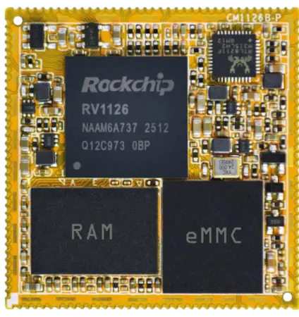
Sistema CM1126B-P integratu Boardcon nantu à u modulu
Specificazioni
| Feature | Specificazioni |
| CPU | Quad-core Cortex-A53 |
| DDR | 2 GB LPDDR4 (finu à 4 GB) |
| eMMC FLASH | 8 GB (finu à 256 GB) |
| putenza | DC 3.3V |
| MIPI DSI | 4-Lane |
| I2S | 4-ch |
| MIPI CSI | 2-CH 4-Lane |
| LCD RGB | 24 bit |
| Camera | 1-CH (DVP) è 2-CH (CSI) |
| USB | 2-CH (USB HOST 2.0 è OTG 2.0) |
| Ethernet | 1000 M GMAC |
| SDMMC | 2-ch |
| I2C | 5-ch |
| SPI | 2-ch |
| UART | 5-CH, 1-CH (DEBUG) |
| PWM | 11-ch |
| ADC IN | 4-ch |
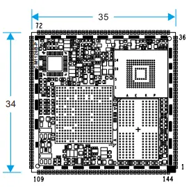
| Dimensione di u bordu | 34 x 35 mm |
Introduzione
Circa stu Manuale
Stu manuale hè destinatu à furnisce l'utilizatori cun un overview di a scheda è i so vantaghji, e specifiche cumplette di e funzioni è e procedure di cunfigurazione. Contene ancu infurmazioni impurtanti nantu à a sicurezza.
Feedback è Actualizazione à stu Manuale
Per aiutà i nostri clienti à sfruttà u massimu di i nostri prudutti, facemu continuamente risorse supplementari è aghjurnate dispunibili nantu à u Boardcon websitu (www.boardcon.com, www.armdesigner.com). Questi include manuali, note d'applicazione, prugrammazione examples, è software è hardware aghjurnatu. Verificate periodicamente per vede ciò chì hè novu! Quandu avemu priurità u travagliu nantu à sti risorse aghjurnati, i feedback da i clienti sò l'influenza numero unu, Sì avete dumande, cumenti, o preoccupazioni nantu à u vostru pruduttu o prughjettu, per piacè ùn esitate à cuntattateci à support@armdesigner.com.
Introduzione à CM1126B-P
Riassuntu
U sistema-nantu-modulu CM1126B-P hè equipatu cù RV1126B-P di Rockchip, custruitu cù un Cortex-A53 quad-core, 3.0 TOPs NPU, è RISC-V MCU. Hè cuncipitu specificamente per i dispositivi IPC/CVR, i dispositivi AI Camera, i dispositivi interattivi intelligenti, è i mini robot. E suluzioni d'altu rendimentu è di bassa putenza ponu aiutà i clienti à introduce nuove tecnulugie più rapidamente è à migliurà l'efficienza generale di a suluzione. A dimensione più chjuca pò esse messa nantu à una scheda 38. Dopu a revisione di l'hardware da CM1126 (V1) à CM1126B-P (V2), induve u SoC hè aggiornatu à RV1126B-P, i signali Reset & OTG_VBUS è u vulume GPIO di u modulu WIFI/BT.tage deve funziunà à un livellu logicu di 3.3V.
Features
Microprocessore
- Quad-core Cortex-A53 finu à 1.6GHz
- 32KB I-cache è 32KB D-cache per ogni core, 512KB L3 cache
- 3.0 TOPS Unità di Prucessu Neurale
- MCU RISC-V per supportà un avvio rapidu di 250 ms
- Max 12 M ISP
Organizazione di a memoria
- RAM LPDDR4 finu à 4 GB
- eMMC finu à 256 GB
- SPI Flash finu à 8 MB
Video Decoder / Encoder
- Supporta a decodificazione / codificazione video finu à 4K @ 30fps
- Supporta a decodificazione in tempu reale di H.264/265
- Supporta a codificazione video UHD H.264/265 in tempu reale
- Dimensione di l'imaghjini finu à 8192 × 8192
Subsistema di visualizazione
- Output Video
- Supporta 4 corsi MIPI DSI finu à 2560 × 1440 @ 60fps
- Supporta l'uscita parallela RGB à 24 bit
- Image in
- Supporta l'interfaccia DVP finu à 16 bit
- Supporta l'interfaccia 2ch MIPI CSI 4lanes
I2S/PCM/AC97
- Tre interfaccia I2S/PCM
- Supporta l'array Mic Finu à l'interfaccia PDM/TDM 8ch
- Supporta l'output audio PWM
USB è PCIE
- Dui interfaccia USB 2.0
- Un USB 2.0 OTG è un host USB 2.0
Ethernet
- RTL8211F à bordu
- Supportu 10/100/1000M
I2C
- Finu à cinque I2C
- Supporta u modu standard è u modu veloce (finu à 400 kbit/s)
SDIO
- Supporta u protocolu 2CH SDIO 3.0
SPI
- Jusqu'à deux contrôleurs SPI,
- Interfaccia seriale sincrona full-duplex
UART
- Supporta finu à 6 UART
- UART2 cù 2 fili per strumenti di debug
- Dui FIFO di 664 byte integrati
- Supporta u modu di cuntrollu di flussu automaticu per UART0/1/3/4/5
ADC
- Finu à quattru canali ADC
- Risoluzione 12-bit
- Voltage gamma di input da 0V à 1.8V
- Supporta finu à 1MS/ssamptarifa di ling
PWM
- 11 PWM in chip cù operazione basatu in interruzzione
- Supporta a facilità di tempu/contatore di 32 bit
- Opzione IR nantu à PWM3/7
Unità di putenza
- Potenza discreta à bordu
- Ingressu unicu 3.3V
Schema di blocchi CM1126B-P
Schema à blocchi RV1126B-P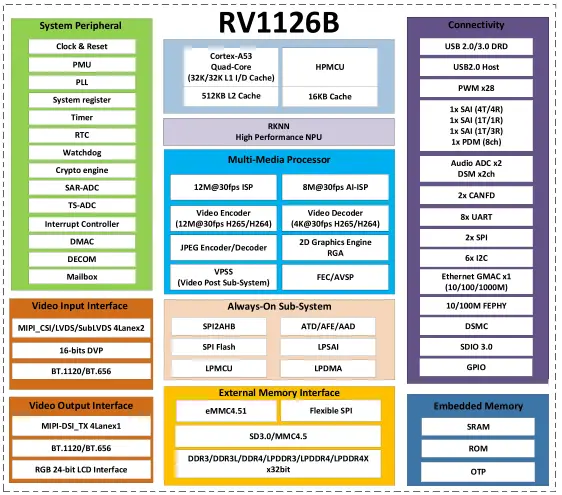
Schema à blocchi di a scheda di sviluppu (Idea1126)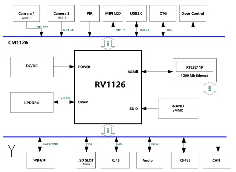
Dimensione di u PCB CM1126B-P
Definizione di u pin CM1126B-P
| Pin | Segnale | Descrizzione o funzioni | GPIO seriale | IO Voltage |
| 1 | LCDC_D19_3V3 | I2S1_MCLK_M2/CIF_D15_M1 | GPIO2_C7_d | 3.3V |
| 2 | LCDC_D20_3V3 | I2S1_SDO_M2/CIF_VS_M1 | GPIO2_D0_d | 3.3V |
| 3 | LCDC_D21_3V3 | I2S1_SCLK_M2/CIF_CLKO_M1 | GPIO2_D1_d | 3.3V |
| 4 | LCDC_D22_3V3 | I2S1_LRCK_M2/CIF_CKIN_M1 | GPIO2_D2_d | 3.3V |
| 5 | LCDC_D23_3V3 | I2S1_SDI_M2/CIF_HS_M1 | GPIO2_D3_d | 3.3V |
| 6 | GND | Terra | 0V | |
| 7 | GPIO1_D1 | UART1_RX_M1/I2C5_SDA_M2 | GPIO1_D1_d | 3.3 V (V2) |
| 8 | BT_WAKE | SPI0_CS1n_M0 | GPIO0_A4_u | 3.3 V (V2) |
| 9 | WIFI_REG_ON | SPI0_MOSI_M0 | GPIO0_A6_d | 3.3 V (V2) |
| 10 | BT_RST | SPI0_MISO_M0 | GPIO0_A7_d | 3.3 V (V2) |
| 11 | WIFI_WAKE_HOST | SPI0_CLK_M0 | GPIO0_B0_d | 3.3 V (V2) |
| 12 | BT_WAKE_HOST | SPI0_CS0n_M0 | GPIO0_A5_u | 3.3 V (V2) |
| 13 | PWM7_IR_M0_3V3 | GPIO0_B1_d | 3.3V | |
| 14 | PWM6_M0_3V3 | TSADC_SHUT_M1 | GPIO0_B2_d | 3.3V |
| 15 | UART2_TX_3V3 | Per debug | GPIO3_A2_u | 3.3V |
| 16 | UART2_RX_3V3 | Per debug | GPIO3_A3_u | 3.3V |
| 17 | I2S0_MCLK_M0_3V
3 |
GPIO3_D2_d | 3.3V | |
| 18 | I2S0_SCLK_TX_M0
_3V3 |
ACODEC_DAC_CLK | GPIO3_D0_d | 3.3V |
| 19 | I2S0_SDI3_M0_3V3 | PDM_SDI3_M0 /
ACODEC_ADC_DATA |
GPIO3_D7_d | 3.3V |
| 20 | I2S0_SDO0_M0_3V
3 |
ACODEC_DAC_DATAR
/APWM_R_M1/ADSM_LP |
GPIO3_D5_d | 3.3V |
| Pin | Segnale | Descrizzione o funzioni | GPIO seriale | IO Voltage |
| 21 | I2S0_LRCK_TX_M0
_3V3 |
ACODEC_DAC_SYNC
/APWM_L_M1/ADSM_LN |
GPIO3_D3_d | 3.3V |
| 22 | PDM_SDI1_3V3 | I2S0_SDO3_SDI1_M0/I2C4SDA | GPIO4_A1_d | 3.3V |
| 23 | PDM_CLK1_3V3 | I2S0_SCK_RX_M0 | GPIO3_D1_d | 3.3V |
| 24 | PDM_SDI2_3V3 | I2S0_SDO2_SDI2_M0/I2C4SCL | GPIO4_A0_d | 3.3V |
| 25 | PDM_SDI0_3V3 | I2S0_SDI0_M0 | GPIO3_D6_d | 3.3V |
| 26 | PDM_CLK_3V3 | I2S0_LRCK_RX_M0 | GPIO3_D4_d | 3.3V |
| 27 | I2C2_SDA_3V3 | PWM5_M0 | GPIO0_C3_d | 3.3V |
| 28 | I2C2_SCL_3V3 | PWM4_M0 | GPIO0_C2_d | 3.3V |
| 29 | USB_HOST_DP | 1.8V | ||
| 30 | USB_HOST_DM | 1.8V | ||
| 31 | GND | Terra | 0V | |
| 32 | OTG_DP | Pò esse adupratu per u scaricamentu | 1.8V | |
| 33 | OTG_DM | Pò esse adupratu per u scaricamentu | 1.8V | |
| 34 | OTG_DET(V2) | OTG VBUS DET IN | 3.3 V (V2) | |
| 35 | OTG_ID | 1.8V | ||
| 36 | SPI0_CS1n_M1 | I2S1_MCK_M1/UART4_TX_M2 | GPIO1_D5_d | 1.8V |
| 37 | VCC3V3_SYS | 3.3V Input Power principale | 3.3V | |
| 38 | VCC3V3_SYS | 3.3V Input Power principale | 3.3V | |
| 39 | USB_CTRL_3V3 | GPIO0_C1_d | 3.3V | |
| 40 | SDMMC0_DET | Deve esse usatu per a carta SD | GPIO0_A3_u | 3.3 V (V2) |
| 41 | CLKO_32K | Output di u clock RTC | GPIO0_A2_u | 3.3 V (V2) |
| 42 | nRESET | Resetta l'input chjave | 3.3 V (V2) | |
| 43 | MIPI_CSI_RX0_CL
KP |
Input MIPI CSI0 o LVDS0 | 1.8V | |
| 44 | MIPI_CSI_RX0_CL
KN |
Input MIPI CSI0 o LVDS0 | 1.8V | |
| 45 | MIPI_CSI_RX0_D2
P |
Input MIPI CSI0 o LVDS0 | 1.8V | |
| 46 | MIPI_CSI_RX0_D2
N |
Input MIPI CSI0 o LVDS0 | 1.8V | |
| 47 | MIPI_CSI_RX0_D3
P |
Input MIPI CSI0 o LVDS0 | 1.8V | |
| 48 | MIPI_CSI_RX0_D3
N |
Input MIPI CSI0 o LVDS0 | 1.8V | |
| 49 | MIPI_CSI_RX0_D1
P |
Input MIPI CSI0 o LVDS0 | 1.8V | |
| 50 | MIPI_CSI_RX0_D1
N |
Input MIPI CSI0 o LVDS0 | 1.8V | |
| 51 | MIPI_CSI_RX0_D0
P |
Input MIPI CSI0 o LVDS0 | 1.8V |
| Pin | Segnale | Descrizzione o funzioni | GPIO seriale | IO Voltage |
| 52 | MIPI_CSI_RX0_D0
N |
Input MIPI CSI0 o LVDS0 | 1.8V | |
| 53 | GND | Terra | 0V | |
| 54 | MIPI_CSI_RX1_D3
P |
Input MIPI CSI1 o LVDS1 | 1.8V | |
| 55 | MIPI_CSI_RX1_D3
N |
Input MIPI CSI1 o LVDS1 | 1.8V | |
| 56 | MIPI_CSI_RX1_CL
KP |
Input MIPI CSI1 o LVDS1 | 1.8V | |
| 57 | MIPI_CSI_RX1_CL
KN |
Input MIPI CSI1 o LVDS1 | 1.8V | |
| 58 | MIPI_CSI_RX1_D2
P |
Input MIPI CSI1 o LVDS1 | 1.8V | |
| 59 | MIPI_CSI_RX1_D2
N |
Input MIPI CSI1 o LVDS1 | 1.8V | |
| 60 | MIPI_CSI_RX1_D1
P |
Input MIPI CSI1 o LVDS1 | 1.8V | |
| 61 | MIPI_CSI_RX1_D1
N |
Input MIPI CSI1 o LVDS1 | 1.8V | |
| 62 | MIPI_CSI_RX1_D0
P |
Input MIPI CSI1 o LVDS1 | 1.8V | |
| 63 | MIPI_CSI_RX1_D0
N |
Input MIPI CSI1 o LVDS1 | 1.8V | |
| 64 | SDMMC0_D3_3V3 | UART3_TX_M1 | GPIO1_A7_u | 3.3V |
| 65 | SDMMC0_D2_3V3 | UART3_RX_M1 | GPIO1_A6_u | 3.3V |
| 66 | SDMMC0_D1_3V3 | UART2_TX_M0 | GPIO1_A5_u | 3.3V |
| 67 | SDMMC0_D0_3V3 | UART2_RX_M0 | GPIO1_A4_u | 3.3V |
| 68 | SDMMC0_CMD_3V
3 |
UART3_CTSn_M1 | GPIO1_B1_u | 3.3V |
| 69 | SDMMC0_CLK_3V3 | UART3_RTSn_M1 | GPIO1_B0_u | 3.3V |
| 70 | GND | Terra | 0V | |
| 71 | LED1/CFG_LDO0 | LED LINK Ethernet | 3.3V | |
| 72 | LED2/CFG_LDO1 | LED SPEED Ethernet | 3.3V | |
| 73 | MDI0 + | Segnale Ethernet MDI | 1.8V | |
| 74 | MDI0- | Segnale Ethernet MDI | 1.8V | |
| 75 | MDI1 + | Segnale Ethernet MDI | 1.8V | |
| 76 | MDI1- | Segnale Ethernet MDI | 1.8V | |
| 77 | MDI2 + | Segnale Ethernet MDI | 1.8V | |
| 78 | MDI2- | Segnale Ethernet MDI | 1.8V | |
| 79 | MDI3 + | Segnale Ethernet MDI | 1.8V | |
| 80 | MDI3- | Segnale Ethernet MDI | 1.8V | |
| 81 | I2C1_SCL | UART4_CTSn_M2 | GPIO1_D3_u | 1.8V |
| Pin | Segnale | Descrizzione o funzioni | GPIO seriale | IO Voltage |
| 82 | I2C1_SDA | UART4_RTSn_M2 | GPIO1_D2_u | 1.8V |
| 83 | MIPI_CSI_PWDN0 | UART4_RX_M2 | GPIO1_D4_d | 1.8V |
| 84 | SPI0_CLK_M1 | I2S1_SDO_M1/UART5_RX_M2 | GPIO2_A1_d | 1.8V |
| 85 | SPI0_MOSI_M1 | I2S1_SCK_M1/I2C3_SCL_M2 | GPIO1_D6_d | 1.8V |
| 86 | SPI0_CS0n_M1 | I2S1_SDI_M1/UART5_TX_M2 | GPIO2_A0_d | 1.8V |
| 87 | SPI0_MISO_M1 | I2S1_LRCK_M1/I2C3_SDA_M2 | GPIO1_D7_d | 1.8V |
| 88 | MIPI_CSI_CLK1 | UART5_RTSn_M2 | GPIO2_A2_d | 1.8V |
| 89 | MIPI_CSI_CLK0 | UART5_CTSn_M2 | GPIO2_A3_d | 1.8V |
| 90 | GND | Terra | 0V | |
| 91 | LCDC_D0_3V3 | UART4_RTSn_M1/CIF_D0_M1 | GPIO2_A4_d | 3.3V |
| 92 | LCDC_D1_3V3 | UART4_CTSn_M1/CIF_D1_M1 | GPIO2_A5_d | 3.3V |
| 93 | LCDC_D2_3V3 | UART4_TX_M1/CIF_D2_M1 | GPIO2_A6_d | 3.3V |
| 94 | LCDC_D3_3V3 | UART4_RX_M1/I2S2_SDO_M1 | GPIO2_A7_d | 3.3V |
| 95 | LCDC_D4_3V3 | UART5_TX_M1/I2S2_SDI_M1 | GPIO2_B0_d | 3.3V |
| 96 | LCDC_D5_3V3 | UART5_RX_M1/I2S2_SCK_M1 | GPIO2_B1_d | 3.3V |
| 97 | LCDC_D6_3V3 | UART5_RTSn_M1/I2S2_LRCK_
M1 |
GPIO2_B2_d | 3.3V |
| 98 | LCDC_D7_3V3 | UART5_CTSn_M1/I2S2_MCLK_
M1/CIF_D3_M1 |
GPIO2_B3_d | 3.3V |
| 99 | CAN_RX_3V3 | UART3_TX_M2/I2C4_SCL_M0 | GPIO3_A0_u | 3.3V |
| 100 | CAN_TX_3V3 | UART3_RX_M2/I2C4_SDA_M0 | GPIO3_A1_u | 3.3V |
| 101 | LCDC_CLK_3V3 | UART3_CTSn_M2/SPI1_MISO_
M2/PWM8_M1 |
GPIO2_D7_d | 3.3V |
| 102 | LCDC_VSYNC_3V3 | UART3_RTSn_M2/SPI1_MOSI | GPIO2_D6_d | 3.3V |
| 103 | MIPI_DSI_D2P | 1.8V | ||
| 104 | MIPI_DSI_D2N | 1.8V | ||
| 105 | MIPI_DSI_D1P | 1.8V | ||
| 106 | MIPI_DSI_D1N | 1.8V | ||
| 107 | MIPI_DSI_D0P | 1.8V | ||
| 108 | MIPI_DSI_D0N | 1.8V | ||
| 109 | MIPI_DSI_D3P | 1.8V | ||
| 110 | MIPI_DSI_D3N | 1.8V | ||
| 111 | MIPI_DSI_CLKP | 1.8V | ||
| 112 | MIPI_DSI_CLKN | 1.8V | ||
| 113 | ADCIN3 | Input ADC | 1.8V | |
| 114 | ADCIN2 | Input ADC | 1.8V | |
| 115 | ADCIN1 | Input ADC | 1.8V | |
| 116 | ADKEY_IN0 | Set di modalità di ricuperazione (10K PU) | 1.8V | |
| 117 | GND | Terra | 0V | |
| 118 | SDIO_CLK | GPIO1_B2_d | 3.3 V (V2) | |
| 119 | SDIO_CMD | GPIO1_B3_u | 3.3 V (V2) |
| Pin | Segnale | Descrizzione o funzioni | GPIO seriale | IO Voltage |
| 120 | SDIO_D0 | GPIO1_B4_u | 3.3 V (V2) | |
| 121 | SDIO_D1 | GPIO1_B5_u | 3.3 V (V2) | |
| 122 | SDIO_D2 | GPIO1_B6_u | 3.3 V (V2) | |
| 123 | SDIO_D3 | GPIO1_B7_u | 3.3 V (V2) | |
| 124 | UART0_RX | GPIO1_C2_u | 3.3 V (V2) | |
| 125 | UART0_TX | GPIO1_C3_u | 3.3 V (V2) | |
| 126 | UART0_CTSN | GPIO1_C1_u | 3.3 V (V2) | |
| 127 | UART0_RTSN | GPIO1_C0_u | 3.3 V (V2) | |
| 128 | PCM_TX | I2S2_SDO_M0/SPI1_MOSI_M1 | GPIO1_C4_d | 3.3 V (V2) |
| 129 | PCM_SYNC | I2S2_LRCK_M0/SPI1_CSn0_M
1/UART1_CTSn_M1 |
GPIO1_C7_d | 3.3 V (V2) |
| 130 | PCM_CLK | I2S2_SCLK_M0/SPI1_CLK_M1/
UART1_RTSn_M1 |
GPIO1_C6_d | 3.3 V (V2) |
| 131 | PCM_RX | I2S2_SDI_M0/SPI1_MISO_M1 | GPIO1_C5_d | 3.3 V (V2) |
| 132 | LCDC_D15_3V3 | CIF_D11_M1 | GPIO2_C3_d | 3.3V |
| 133 | LCDC_D14_3V3 | CIF_D10_M1 | GPIO2_C2_d | 3.3V |
| 134 | LCDC_D13_3V3 | CIF_D9_M1 | GPIO2_C1_d | 3.3V |
| 135 | LCDC_D12_3V3 | CIF_D8_M1 | GPIO2_C0_d | 3.3V |
| 136 | LCDC_DEN_3V3 | I2C3_SCL_M1/SPI1_CS0n_M2 | GPIO2_D4_d | 3.3V |
| 137 | LCDC_D10_3V3 | CIF_D6_M1 | GPIO2_B6_d | 3.3V |
| 138 | LCDC_D9_3V3 | CIF_D5_M1 | GPIO2_B5_d | 3.3V |
| 139 | LCDC_D8_3V3 | CIF_D4_M1 | GPIO2_B4_d | 3.3V |
| 140 | LCDC_D11_3V3 | CIF_D7_M1 | GPIO2_B7_d | 3.3V |
| 141 | LCDC_HSYNC_3V3 | I2C3_SDA_M1/SPI1_CLK_M2 | GPIO2_D5_d | 3.3V |
| 142 | LCDC_D16_3V3 | CIF_D12_M1 | GPIO2_C4_d | 3.3V |
| 143 | LCDC_D17_3V3 | CIF_D13_M1 | GPIO2_C5_d | 3.3V |
| 144 | LCDC_D18_3V3 | CIF_D14_M1 | GPIO2_C6_d | 3.3V |
| Nota:
1. Most GPIO voltage hè 1.8V, ma certi pin marcati 3.3V. 2. GPIO vulumetagCambiate à 3.3V per marcatu (V2). |
||||
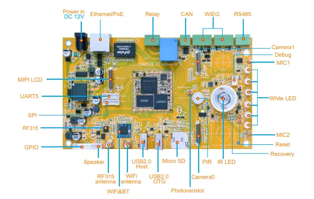
Kit di Sviluppu (Idea1126)
Guida di cuncepimentu di hardware
Riferimentu di u circuitu perifericu
Circuitu di putenza principale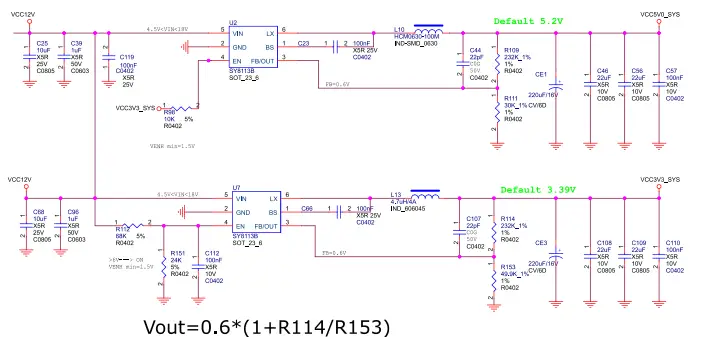
Debug Circuit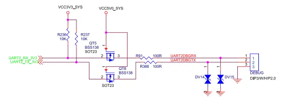
Circuitu d'interfaccia USB OTG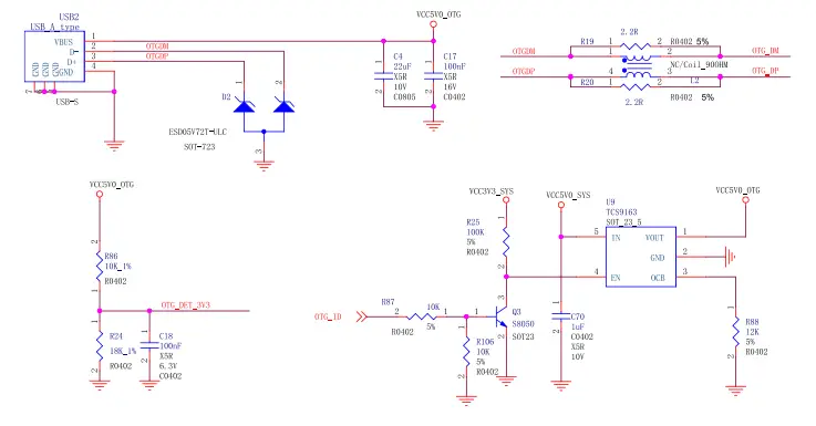
Impronta PCB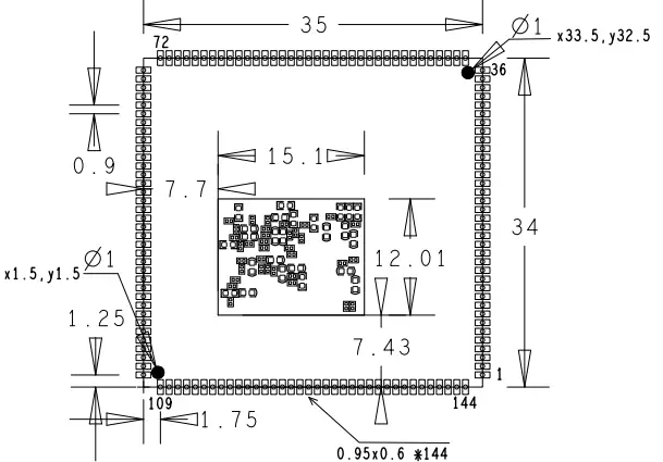
Caratteristiche elettriche di u produttu
Dissipazione è Temperature
| Simbulu | Parametru | Min | Tipu | Max | Unità |
| VCC3V3_SYS | Sistema IO
Voltage |
3.3-5% | 3.3 | 3.3 + 5% | V |
| Isys_in | VCC3V3_SYS input Current | 850 | mA | ||
| Ta | Temperature di funziunamentu | -20 | 70 | °C | |
| Tstg | Temperature di almacenamiento | -40 | 85 | °C |
Affidabilità di a prova
| Test di operazione à alta temperatura | ||
| Cuntenuti | Funziunamentu 8 ore à alte temperature | 55 ° C ± 2 ° C |
| Risultatu | TBD |
| Test di vita operativa | ||
| Cuntenuti | Funziunendu in a stanza | 120 ore |
| Risultatu | TBD |
Garanzia limitata
Boardcon garantisce chì stu pruduttu hè senza difetti di materiale è di fabricazione per un annu da a data di compra. Durante stu periodu di garanzia, Boardcon riparerà o rimpiazzerà l'unità difettosa per mezu di u prucessu seguente: Una copia di a fattura originale deve esse inclusa quandu si restituisce l'unità difettosa à Boardcon. Sta garanzia limitata ùn copre micca i danni risultanti da fulmini o altre sovratensioni, usu impropriu, abusu, cundizioni anormali di funziunamentu, o tentativi di alterà o mudificà a funzione di u pruduttu. Sta garanzia hè limitata à a riparazione o a sustituzione di l'unità difettosa. In nessun casu Boardcon serà rispunsevule di alcuna perdita o dannu, cumpresi, ma senza limitazione à, qualsiasi perdita di profitti, danni incidentali o consequenziali, perdita di affari, o profitti anticipati derivanti da l'usu o l'incapacità di utilizà stu pruduttu. E riparazioni effettuate dopu a scadenza di u periodu di garanzia sò sottumesse à una spesa di riparazione è à u costu di spedizione di ritornu. Per piacè cuntattate Boardcon per urganizà qualsiasi serviziu di riparazione è per ottene informazioni nantu à a spesa di riparazione.
FAQs
D: Cumu possu aghjurnà a memoria DDR nantu à CM1126B-P?
A: U CM1126B-P supporta finu à 4 GB di memoria LPDDR4. Per l'aghjurnamentu, assicuratevi di a cumpatibilità cù e specifiche è seguitate e procedure raccomandate.
D: Chì ghjè u bisognu di alimentazione per CM1126B-P?
A: L'alimentazione necessaria per CM1126B-P hè DC 3.3V. Assicuratevi di furnisce una alimentazione stabile in questu intervallu per una prestazione ottimale.
D: Possu allargà a capacità di almacenamiento di eMMC nantu à CM1126B-P?
A: Iè, u almacenamentu eMMC nantu à CM1126B-P pò esse allargatu finu à 256 GB. Assicuratevi a cumpatibilità cù i dispusitivi di almacenamentu supportati prima di l'aghjurnamentu.
Documenti / Risorse
 |
Sistema CM1126B-P integratu Boardcon nantu à u modulu [pdfManuale d'usu V2.20250422, CM1126B-P Sistema nant'à Modulu, CM1126B-P, Sistema nant'à Modulu, Modulu |